AMD Helios and MI350 Offer Hope for the NIC, PCIe Retimer, and PCIe Switch Markets
AMD's next-gen platforms offer a ripe playground for those snubbed by NVIDIA
AMD recently offered a glimpse into its future at the AMD Advancing AI 2025 event in San Jose, California. With the launch of the AMD Instinct MI350 series, the company showed a platform in 2025 that not just offered something new in the space, but also offered an opportunity to companies like Astera Labs in the PCIe Retimer markets and Broadcom in the PCIe switch markets. Looking to the future 2026 platform, the AMD Helios and MI400 platforms seem to offer a similar opportunity.
AMD Helios and MI350 Offer Hope for the NIC, PCIe Retimer, and PCIe Switch Markets
As a quick recap, we recently showed how in both the PCIe GPU and in the SXM-based HGX platforms NVIDIA was actively designing out NICs, PCIe switches, and retimers in what appears to be a targeted effort to remove Broadcom and others from NVIDIA’s 2H 2025 platforms. You can check those pieces in:
NVIDIA B300 SXM/ HGX Segment
AMD, however, is taking a more traditional approach, and perhaps a more conservative and open approach to its architecture. That seems to spell opportunity for companies like Broadcom, Astera Labs, and Marvell.
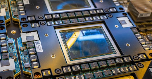
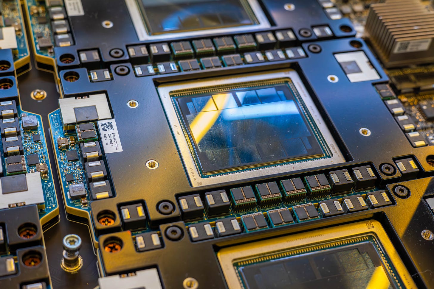
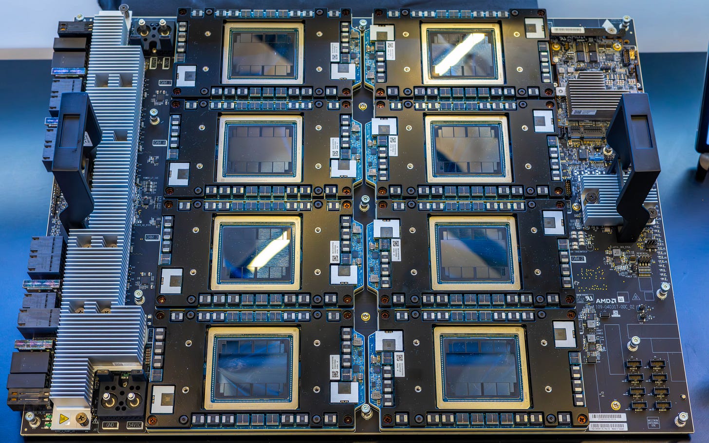
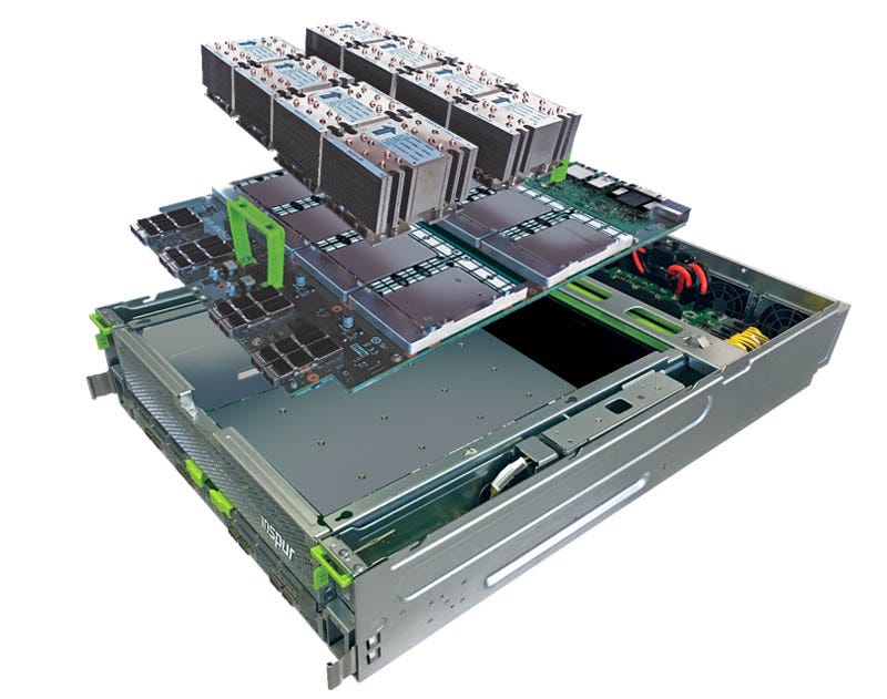
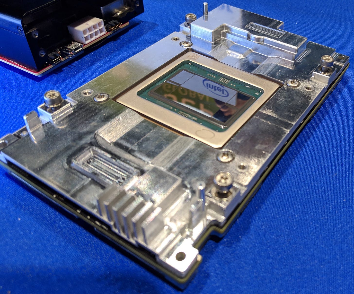
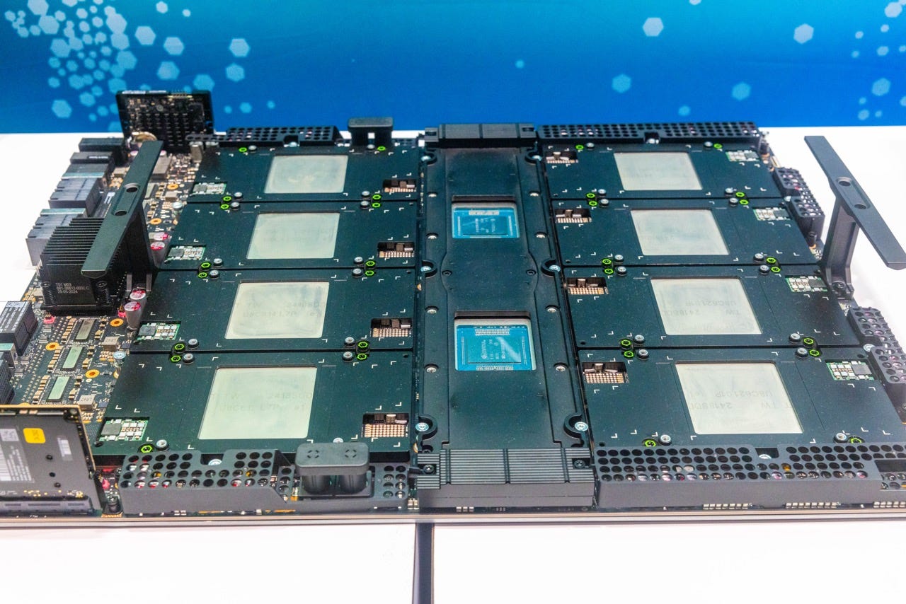
Taking a quick look at the AMD Instinct MI350X/ MI355X boards, one can see that we have an 8-GPU universal baseboard (UBB) design. As some background, UBB was originally designed in the late 2010s as a universal platform for various forms of accelerators, including GPUs and AI accelerators. The corresponding format for packages to install into UBB was the OAM or open accelerator module.
To give you some sense, AMD uses OAM, but we have seen custom accelerators, three different Intel GPU/ AI accelerator architectures using OAM, and even FPGAs in OAM. Initially, the large hyper-scalers wanted OAM and UBB to push NVIDIA away from proprietary HGX platforms. The idea was to have an 8-way baseboard that provided host connections and interconnects between all eight accelerators. Some of the benefits of having one baseboard were driving up volumes to increase quality, flexibility for hyper-scalers in accelerated platform designs, and lower costs for companies building eight accelerator systems.
OAM and UBB have seen many accelerators that used them fail, or fail to gain market traction over the years, and that probably speaks to why the platform is great. Instead of each failed accelerator wasting resources on designing its own eight-way platform from scratch, those efforts were largely saved.
Still, between NVIDIA HGX 8-GPU platforms, AMD Instinct MI300X, and more, UBB has succeeded in one area: the connections.
While NVIDIA decided not to adopt the OAM specification, instead keeping SXM and NVLink, it managed to keep its HGX 8-GPU platforms following UBB dimensions and, importantly, the UBB power and data (PCIe) connections. Effectively, NVIDIA’s answer to the late 2010’s hyper-scalers call for standardized UBB and OAM, was to build the assemblies to fit within the same enclosures, but to take ownership of the entire baseboard through accelerator design.
The basic architecture that you see on various UBB servers is that there are eight PCIe retimers to help maintain the link across the UBB connectors to the system, including the NVIDIA HGX B200 board shown above and below. On the system side of the connectors, there are PCIe switches.
In the late 2025 NVIDIA HGX B300 generation, this is largely going to change, but AMD’s MI350X and MI355X will still leverage this model. Let us dig into that a bit more.

