


NVIDIA Just Ended Broadcom's Chances in a Traditional AI Segment with This
$4000+ of BOM Opportunity Locked Out

At Computex 2025, one announcement sent shockwaves through the AI server industry. NVIDIA updated the 8-GPU PCIe designs with a new reference board that totally changed how future 8-GPU PCIe servers will be built. For server OEMs/ ODMs, this was universally seen as a way to curtail their efforts to differentiate. For Broadcom and, to some extent, Astera Labs, this effectively is locking out a market for their products. It also provides a capability that will be important when we start to see next-generation GPUs from NVIDIA arrive later in 2025. As such, it seems like a good idea to get into what was announced and what is being impacted.
The New NVIDIA ConnectX-8 GPU Board
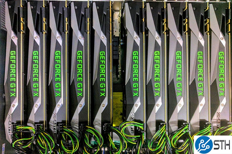
If you were to go back in STH archives to 2015, you would have seen a number of 8-GPU PCIe servers. That was a time before the NVLink switches were out, and the go-to model for deep learning research was cramming 8-10 NVIDIA GeForce cards into a server. By 2017, that had moved to the GeForce GTX 1080 Ti generation, and we started seeing some massive systems that utilized Mellanox cards for relatively low-end interconnect. Even back then, we saw deployments of hundreds and thousands of GPUs all using a similar architecture.
The basic architecture was to have PCIe lanes from the Intel Xeon CPUs connect to a PCB that had both the PCIe slots for the GPUs, as well as Broadcom PCIe switches. In the 2017 era, before NVLink and many of the scale-out (NCCL) technologies really took hold, an advantage of this was that a company could decide to use a single PCIe root complex where GPU-to-GPU communication would occur solely across the PCIe switch board. This allowed P2P traffic to occur between the GPUs without having to to all the way to the CPUs and potentially slow socket-to-socket links.
The other option, and the one that ultimately became more common, was to have multiple sets of PCIe switches, and those PCIe switches to be connected to a few GPUs and both CPUs. NVIDIA restricted NCCL on GeForce, forcing customers to buy higher-end cards, but in the process made using multiple PCIe switches much more palatable.

If you want to see what an example of a multiple GPU PCIe board was back in 2017, here is a look.
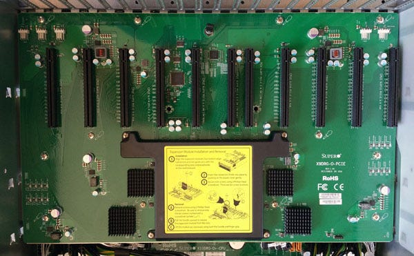
Here is a basic block diagram of a PCIe Gen3 era GPU server we reviewed from Supermicro. As you can see, the four PEX8747 PCIe switches each connected to the CPU and two GPUs. There were then additional slots for NICs and other expansion such as for storage.
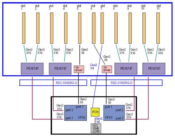
PEX is a name that goes back to the old PLX days. PLX was purchased by Avago, then became Broadcom. Component prices skyrocketed with the acquisition, and that actually had a notable impact on all-NVMe flash storage adoption in the industry. Microsemi/ Microchip had another line of switches, but it has not been competitive in recent generations. Instead, we have seen upstarts like Astera Labs come into this market with its PCIe switches usually having four switches on the PCIe daughterboard.
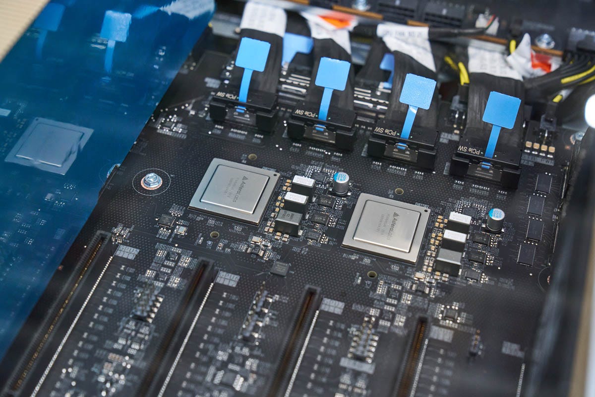
Just to give you some sense of progress over the past 8 years, we reviewed an ASUS 8x PCIe GPU server recently. Here is the block diagram for that, whit the note that the DDR5 links should be to the CPU, not the PCIe switches. A similar idea of the switched architecture utilizing multiple PCIe (Gen5) x16 roots on each CPU and then the PCIe switches connecting to multiple GPUs is still in play.
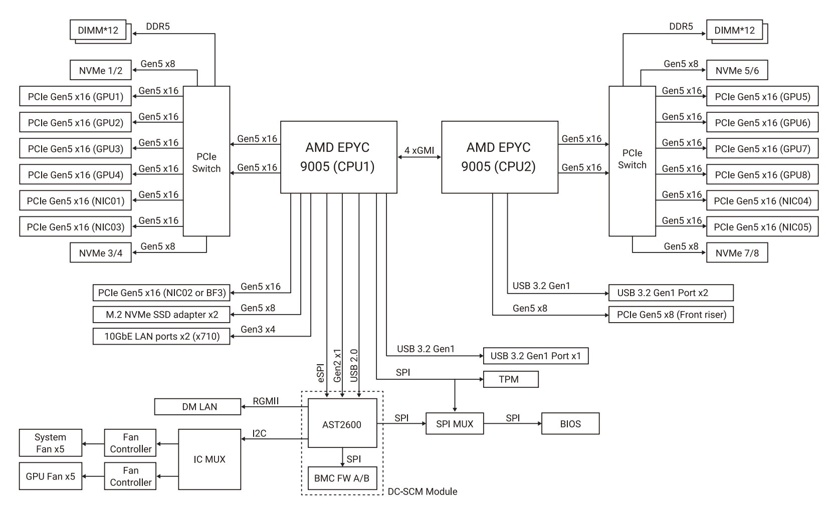
Here, there are some very important points to make. Namely, the NICs have migrated over the years from being attached to the CPUs to being attached to the PCIe switches. That configuration allows for direct GPU to NIC communication without having to traverse the CPU and its PCIe root complexes. The number of NICs has also increased from perhaps one in a system to one for every two GPUs. In this configuration, we have NVMe storage on the PCIe switches just like we would see in a HGX 8-GPU platform for GPUDirect storage.